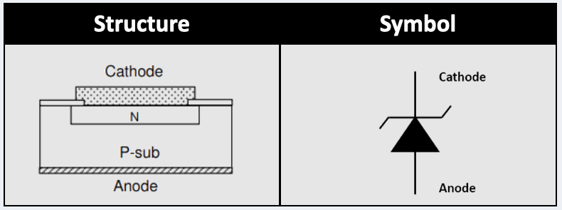
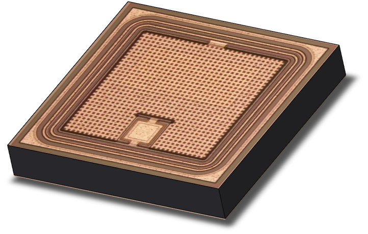
パワーMOSFET
TASCのパワーMOSFETは優れた耐圧能力と低抵抗性を持つだけでなく、高速スイッチング特性を持つため、高効率の電力変換を実現することが可能です。電源変換器、照明制御、直流モータ制御、電子ロック、充電器、力率調整装置等のソリューションとして、小電力から大電力までの各種用途シーンで使用が可能です。多くのグローバルメーカーにとって差別化された製品の需要を満たすための理想的な選択です。
Mechanism
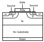
Vertical Double Diffused MOSFET is also called VD-MOSFET ;The distinguishing feature of VD-MOSFET is its vertical P-N junction structure, which gives it excellent voltage withstand capability and low resistance. In VD-MOSFET, charge is vertically diffused into the N-channel region and it can operate at lower drain voltages, making it an ideal choice for many high-power applications.


Main application
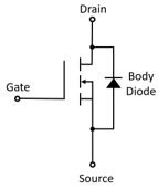
In addition to its high voltage withstand capability, VD-MOSFET also possesses fast switching characteristics, enabling efficient power conversion. During switching operations, VD-MOSFET can transit between high-resistance and low-resistance states in a very short time, thereby improving overall system efficiency. Furthermore, VD-MOSFET offers low static power consumption and high reliability, making it suitable for a wide range of applications.
Power Converter
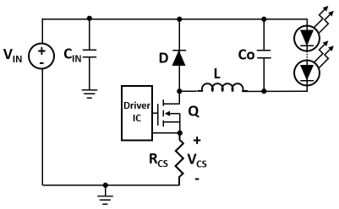
Lighting Control
The main applications of VD-MOSFET include power converters, lighting control, DC motor control, electronic locks, chargers, wireless chargers, and power factor correctors. In these applications, VD-MOSFET can provide efficient power conversion and reliability while meeting the requirements for high voltage and low resistance. As a result, it finds widespread use and favor in many high-power applications.
Key parameters for MOSFET application
When using MOSFETs, it is important to consider insulation, heat dissipation, electrostatic protection, and good circuit design. In designing MOSFET circuits, factors such as input power, load, and control circuits need to be considered to ensure the proper functioning of the entire system. Additionally, it is necessary to select and configure other electronic components such as diodes and capacitors appropriately. When using MOSFETs, it is necessary to understand their important parameters, such as:
-
Absolute Maximum Ratings :
– BVDSS (Drain-Source Breakdown Voltage) : Maximum breakdown voltage between drain and source.
– VGSS (Gate-Source Voltage) : Maximum driving voltage between gate and source.
– ID(max) (Continuous Drain current (max.) : Maximum continuous drain current.
– PD (Power Dissipation) : Maximum power dissipation of the MOSFET.
– Tj (Operating Junction Temperature) : Maximum operating junction temperature of the MOSFET.
-
Electricity Characteristic :
– RDS(on) (Drain to Source on Resistance) : On-resistance of the drain-source channel.
– IDSS (Drain to Source Leakage Current) : Leakage current between drain and source.
– IGSS (Gate to Source Leakage Current) : Leakage current between gate and source.
– Vth (Gate threshold Voltage) : MOSFET turn-on voltage or gate threshold voltage.
– VSD (Diode forward voltage drop) : Parasitic diode forward voltage drop.
-
Dynamic Parameters :
– Ciss (Input Capacitance) : Input power capacitance
The total capacitance of Cgs (gate-source capacitance) and Cgd (gate-drain capacitance).
– Coss (Output Capacitance) : Output power capacitance
The total capacitance of Cds (drain-source capacitance) and Cgd (gate-drain capacitance), and it represents all the capacitance on the output power side.
– Crss (Reverse Transfer Capacitance) : Feedback capacitance
Cgd (gate-drain capacitance)
-
Transfer Switch Parameters :
– Qg (Total Gate Charge):
The amount of gate charge required for the MOSFET to transit from 0V gate voltage to a certain voltage during operation, which is charged by Ciss (input capacitance).
– Qgs (Gate to Source Charge):
The amount of charge between the gate and source needed for the gate voltage to rise from 0V to a certain voltage, charged by the gate-to-source capacitance.
– Qgd (Gate to Drain Charge):
The amount of charge between the gate and drain needed for the drain-to-source voltage (VDS) to drop from the supply voltage to the on-state voltage, charged by the gate-to-drain capacitance.
– Tr (Rising Time):
The time required for the drain-to-source voltage to decrease from 90% of the setting voltage to 10%.
– Td(on) (Turn On Delay Time):
The time from the gate-to-source voltage drops to 90% of the setting voltage to the drain-to-source voltage rises to 10% of the setting voltage.
– Tf (Falling Time):
The time required for the drain-to-source voltage to rise from 10% to 90% of the setting voltage.
– Td(off) (Turn Off Delay Time):
The time from the gate-to-source voltage drops to 90% of the setting voltage to the drain-to-source voltage rises to 10% of the setting voltage.