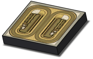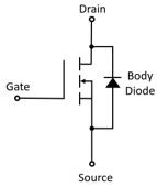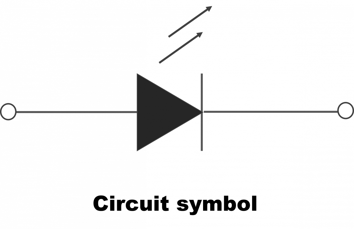
フォトダイオード
台亜製のフォトダイオードは性能、技術、品質において先頭に立っています。検出用途のために、アプリケーションニーズを合わせて製品を生産してきます。40年近くの業界経験及び継続的な革新によって、TASC PDはウェアラブル、コンシューマ、車載、セキュリティー、工業や家電製品などの分野に満たして、お客様へビジネスチャンスを作ります。
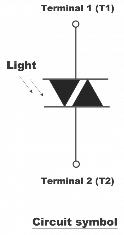
Mechanism
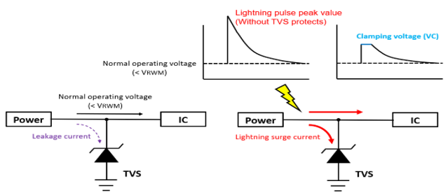
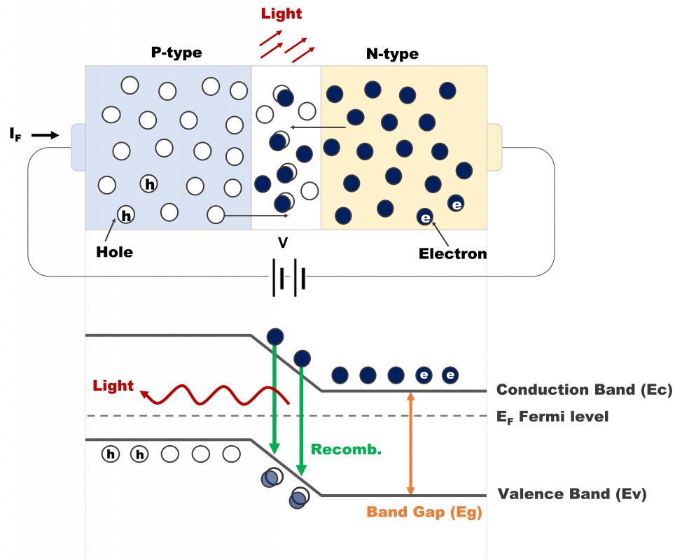
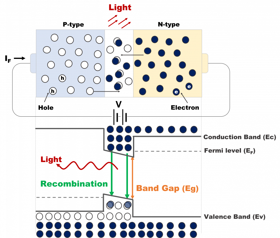
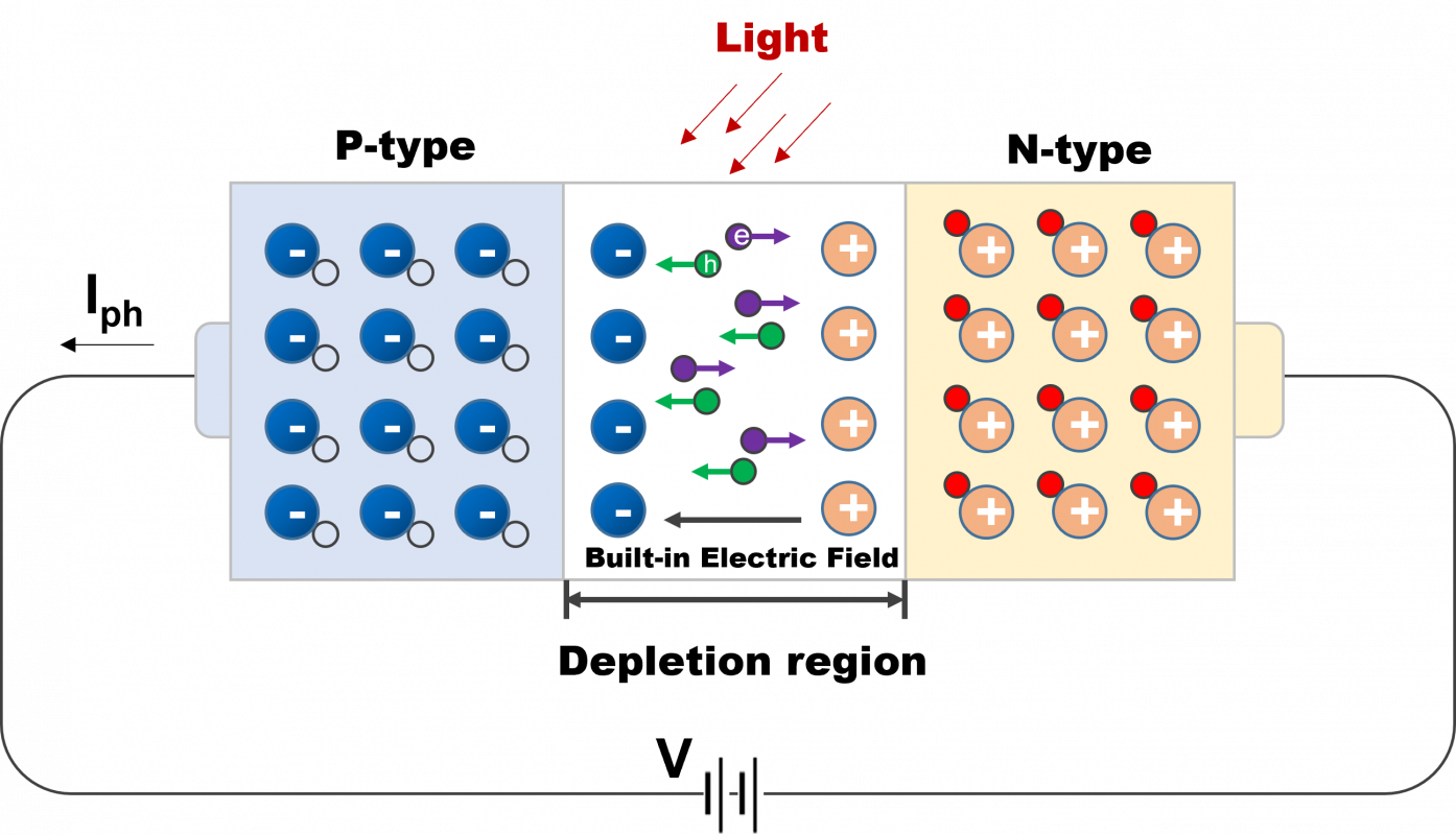
When an equipped with enough energy photon hit the photodiode and the absorption occurs in the depletion region, the built-in electric field will make the electron-hole pair move toward the anode and the cathode to generate the photo current. In fact, the light signal is the sum of the photo current and dark current. Thus, the dark current regarded as a noise should be effectively reduced to increase the sensitivity on the device.
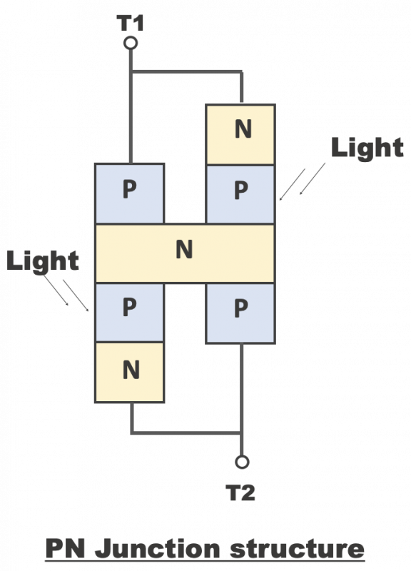
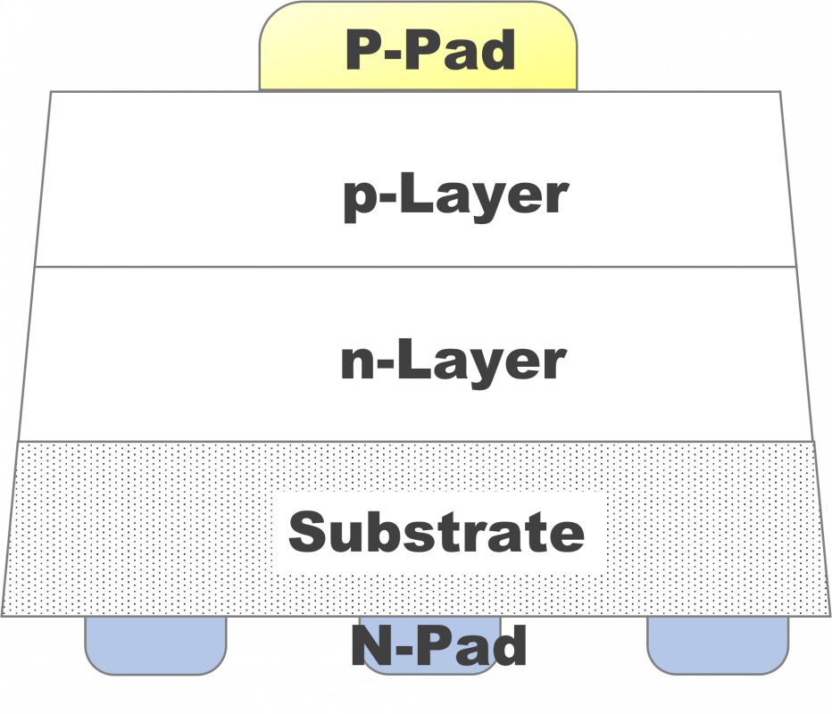
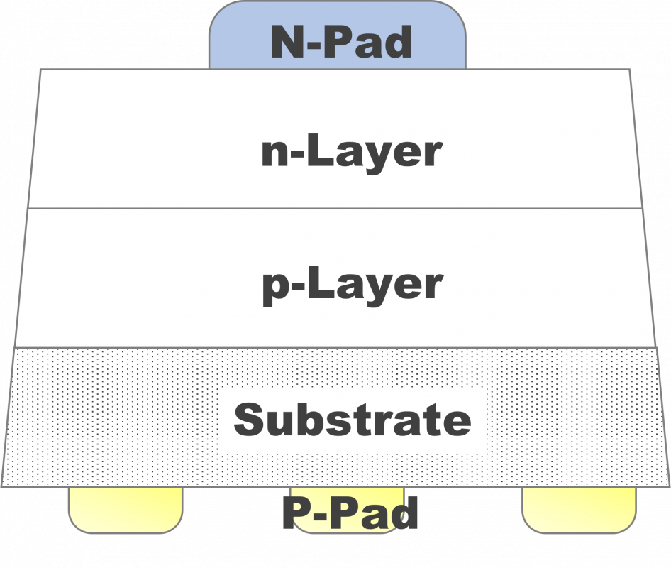
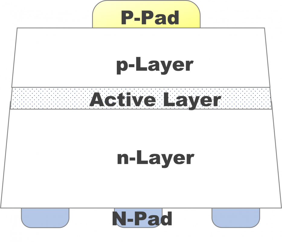
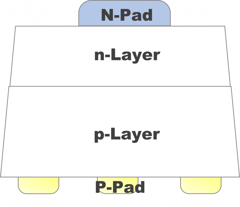
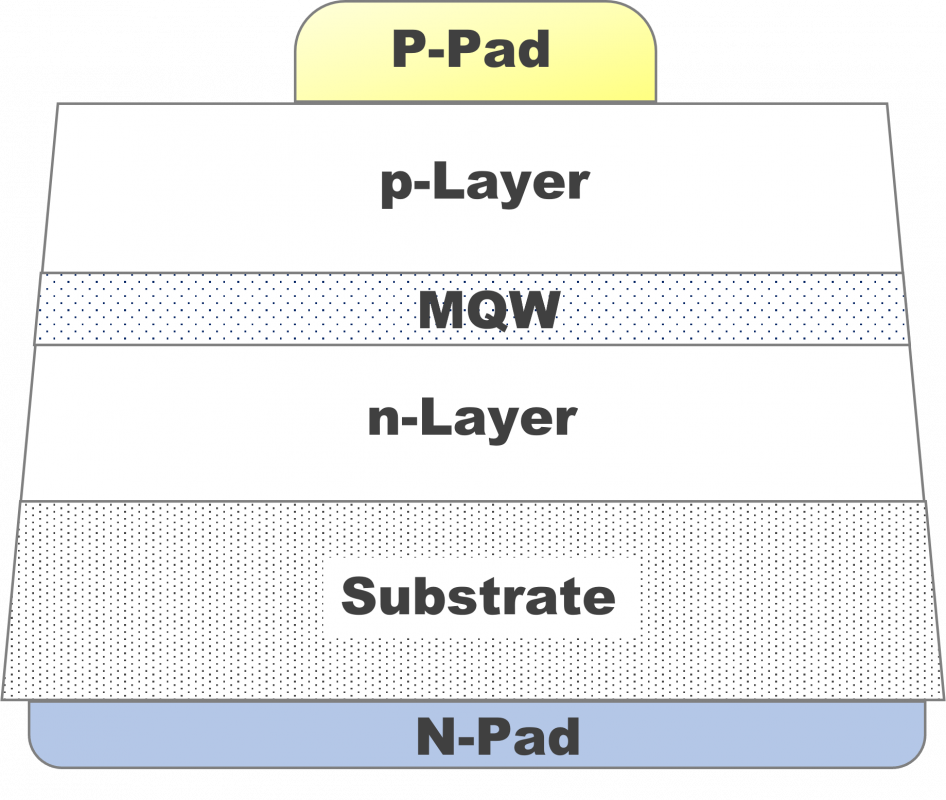
Device Structure
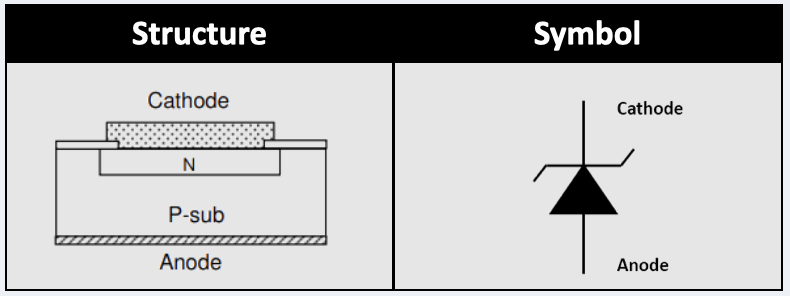
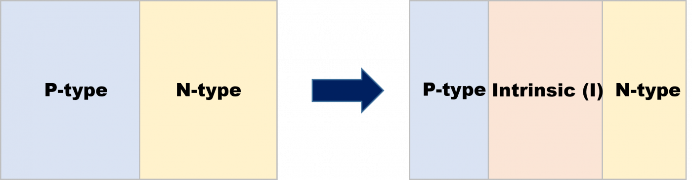
The photodiode is composed of PN junction. Inserting the intrinsic layer with high resistivity will form the PIN structure which increase the effective width of depletion layer. Apart from increasing the breakdown voltage, it also generates large amount of electron-hole pair to increase quantum efficiency. Moreover, it further reduces the junction capacitance to raise device switching speed.
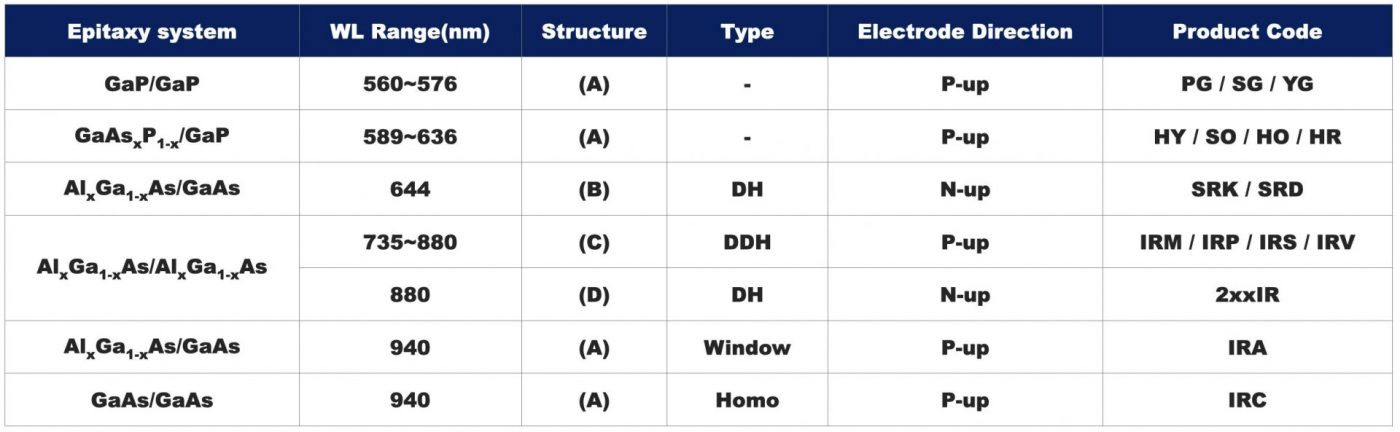
Material selection
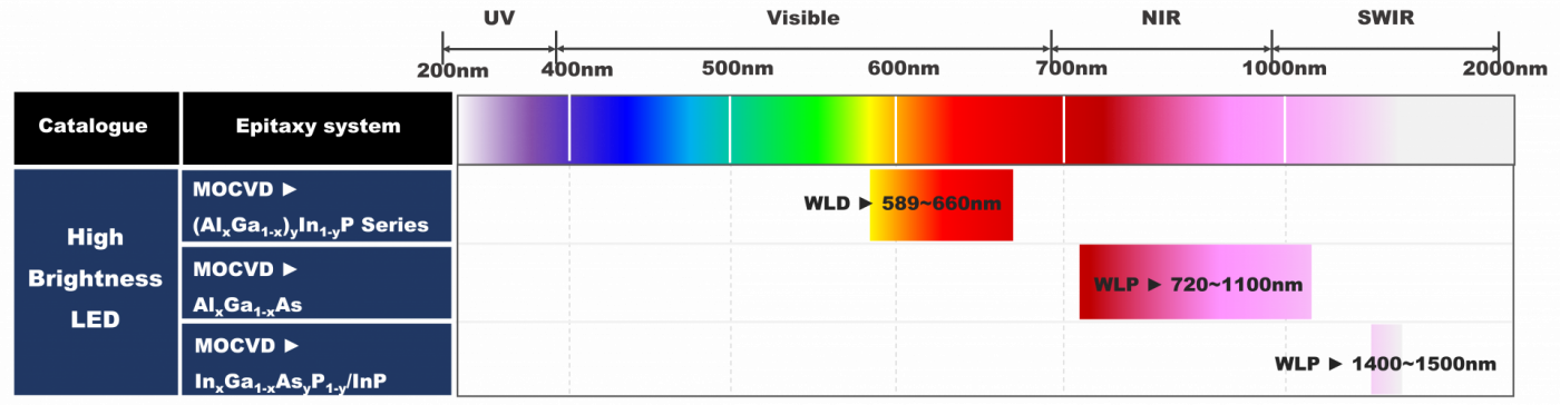
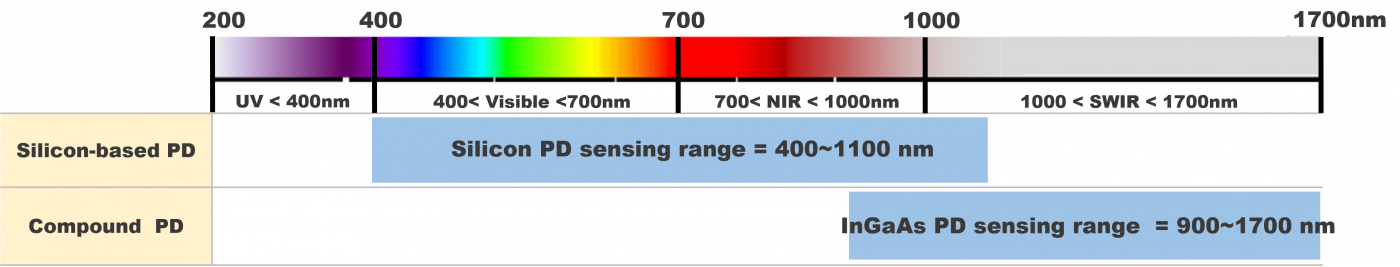
Because the photodiode is sensitive to particular wavelength range, so according to wavelength of light source, the corresponding materials will be chosen to do detection. The materials shown below :
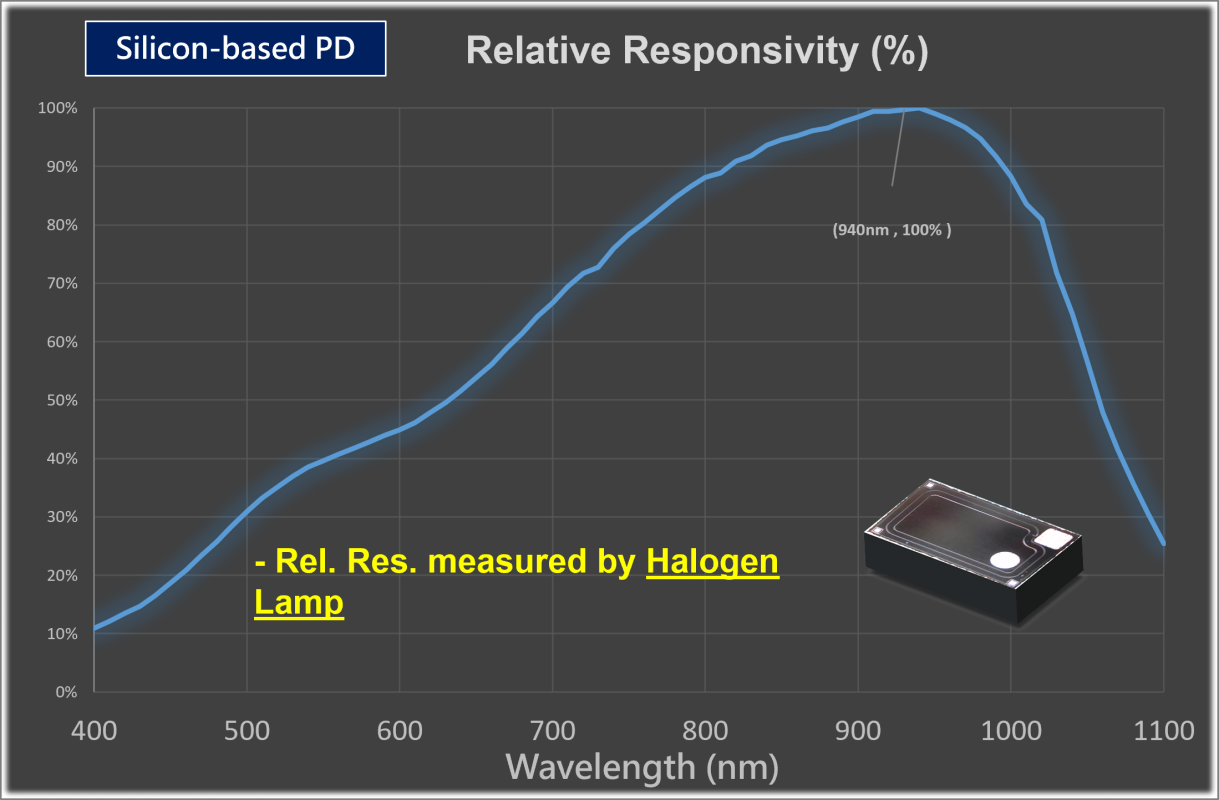
Silicon-based PD : Common sensing wavelength within 400~1100 nm
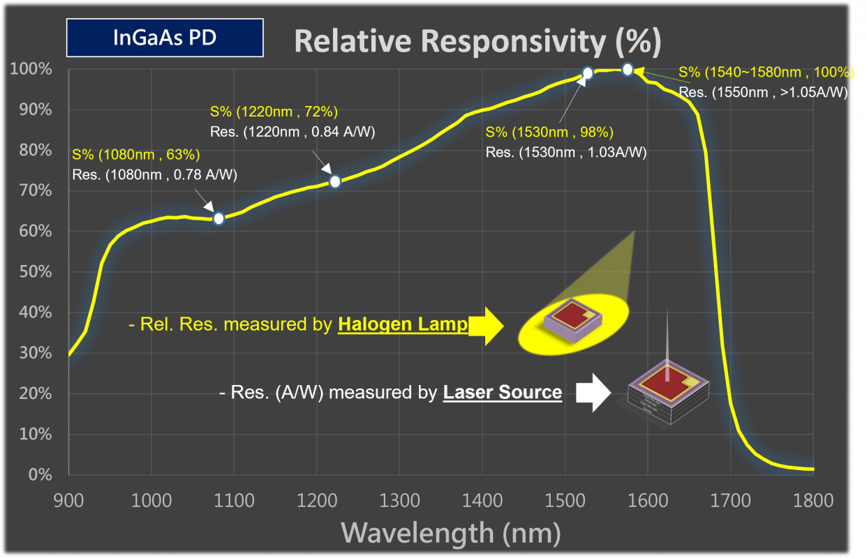
Compound PD : InGaAs PD, common sensing wavelength within 900~1700nm
Characteristics
Responsivity : The conversion efficiency between radiant optical power and the generated current ; The unit is Ampere/Watt (A/W), which can also be converted to quantum efficiency (%)
Dark current : The internal flowing current in the optical sensing device with no incident light environment ; The unit is nA
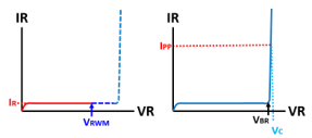
Breakdown Voltage : The minimum reverse bias voltage when diode reverse conducting
Responsivity spectrum : The line diagram of photocurrent conversion efficiency over different wavelength of incident light source. The light spectral shown as below :